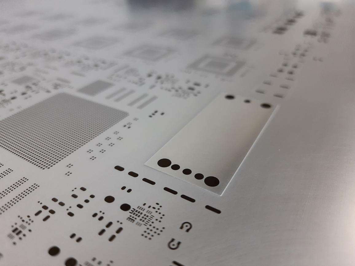
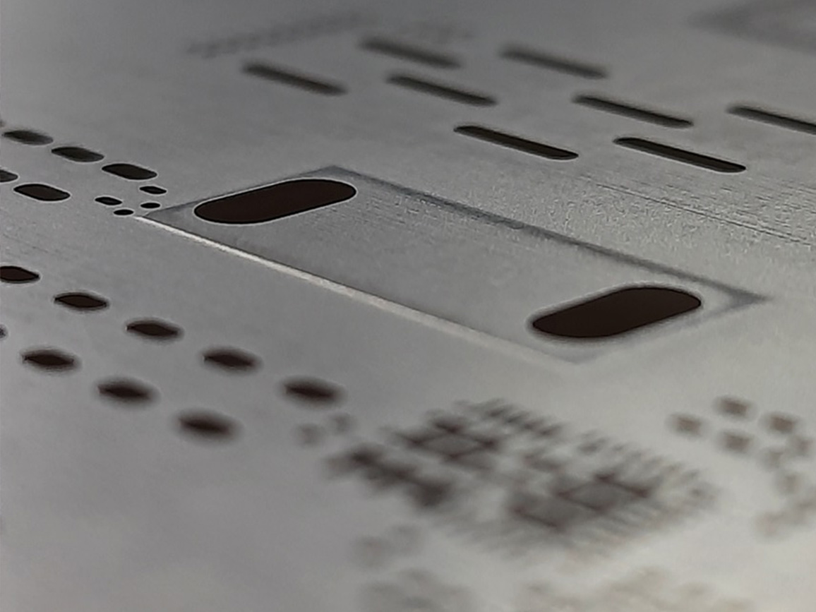
A step stencil provides enhanced flexibility by allowing different stencil thicknesses within a single design. This enables precise control of solder paste volume, ensuring optimal PCB planarity during a single printing process.
Precision Where it Matters
- Step-Down Areas
Reduced stencil thickness for fine-pitch components, minimizing solder paste volume to prevent bridging and improve print accuracy. - Step-Up Areas
Increased stencil thickness for selected components, delivering higher solder paste volume to ensure reliable joint formation.
Engineered for Performance
Our experienced design team carefully evaluates your PCB layout and specifications to develop a multi-layered step stencil that delivers optimal performance, consistency, and yield.
Performance Advantages of Multi-Layered Step Stencils
Improved Print Accuracy
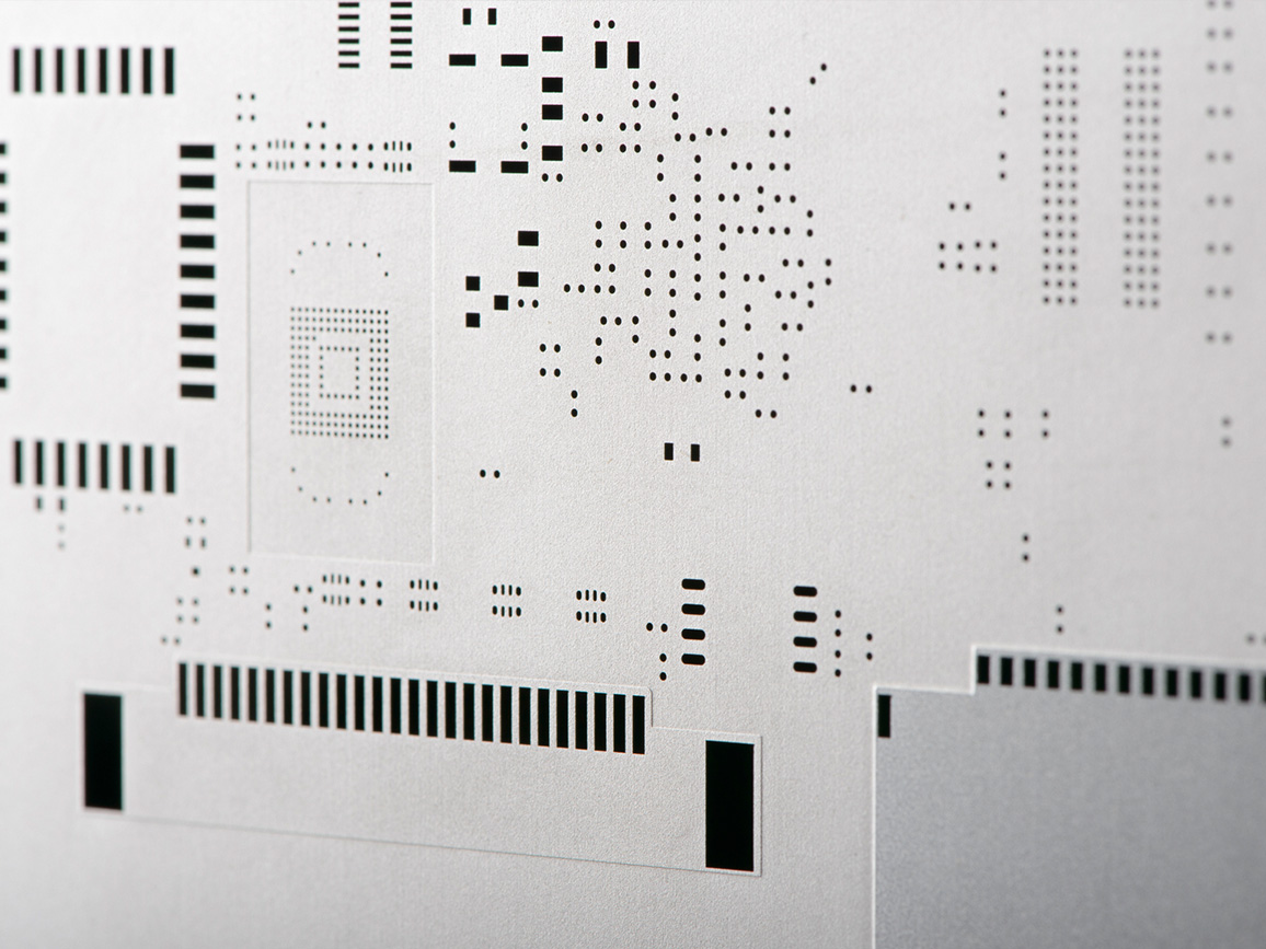
Controlled stencil thickness ensures precise solder paste deposition, especially for fine-pitch and high-density components.
Reduced Solder Defects
Minimizes common issues such as bridging, insufficient solder, and tombstoning through optimized paste volume control.
Enhanced Joint Reliability
Delivers the right amount of solder where needed, resulting in stronger, more consistent solder joints.
Optimized PCB Planarity
Balances solder height across components, improving overall board flatness and assembly quality.
Higher Production Yield
Reduces rework and defects, leading to more stable and efficient manufacturing output.
Greater Design Flexibility
Supports mixed component sizes and complex PCB layouts within a single stencil solution.