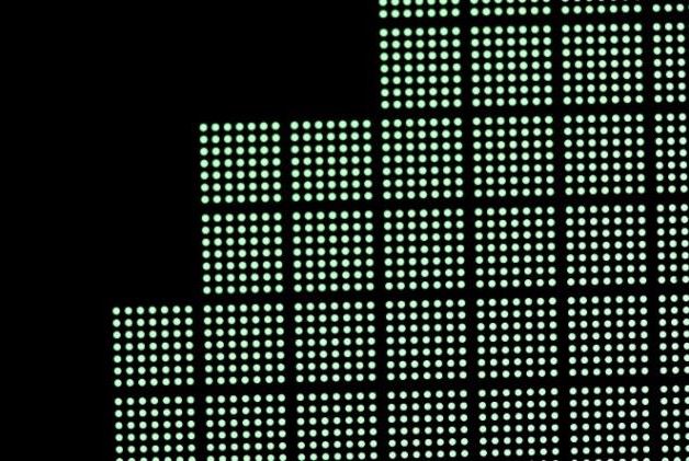
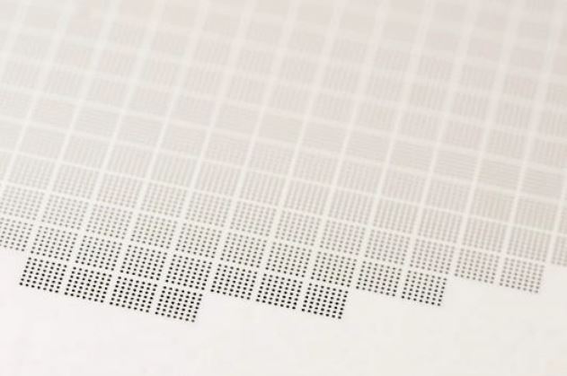
Electroformed stencil aperture walls are extremely smooth—almost mirror-like—which significantly reduces the surface area available for solder paste adhesion. This smooth surface allows solder paste to release more cleanly and consistently during the printing process, improving overall print performance.
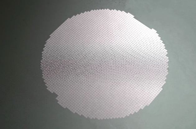
Unlike laser-cut stencils, electroformed SMT stencils are manufactured through a nickel deposition (electroforming) process. Nickel is built up around a precision photoresist template that defines the aperture geometry. This template is created directly from the PCB design, enabling extremely accurate reproduction of fine and complex features.
Key Advantages of Electroformed Stencils:
Ultra-smooth aperture walls for superior solder paste release
More consistent solder volume transfer across all apertures
High precision for fine-pitch and micro components
Improved print performance for advanced SMT applications
Electroformed stencils are especially suited for ultra-fine pitch devices, high-density PCB designs, and applications requiring exceptional print accuracy and consistency.