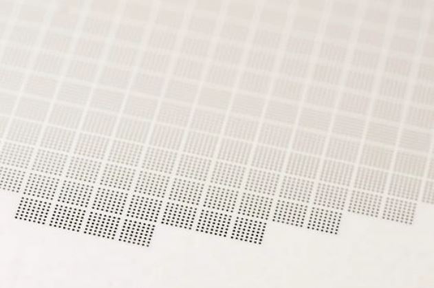
Electroformed stencil aperture walls are extremely smooth (almost mirror-like), which reduces the surface area available for solder paste to adhere to. Because of this, solder paste releases more cleanly and consistently during printing.
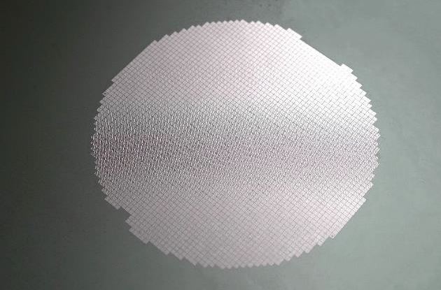
Unlike laser-cut stencils, electroformed stencils are manufactured by depositing nickel through an electroforming process around a photoresist template that defines the aperture pattern. This template is created to precisely match the PCB design, allowing very accurate and fine-feature apertures.
The result is:
Smoother aperture walls → better paste release
More consistent solder volume deposits
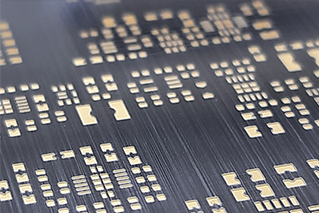
Improved performance for fine-pitch and ultra-small components